System/1 Build Log
An ongoing chronology of System/1's construction, and any other related musings.
7th February, 2015 - More memory interface testing
The dreaded Real Life has kept me away from the tinkering bench lately, but I have managed to find the odd spare hour to get on with testing the memory interface.
First up was a simple set of walking-bit tests to make sure that all the address and data lines behave as expected; the hardest part of that escapade was wiring up 64 channels of the logic analyser, especially since a previous owner of the machine had neglected to label 32 of the flying probe leads before bundling them together into seemingly-arbitrary bunches. Argh. However, after identifying each of them and hooking them all up, away we went:
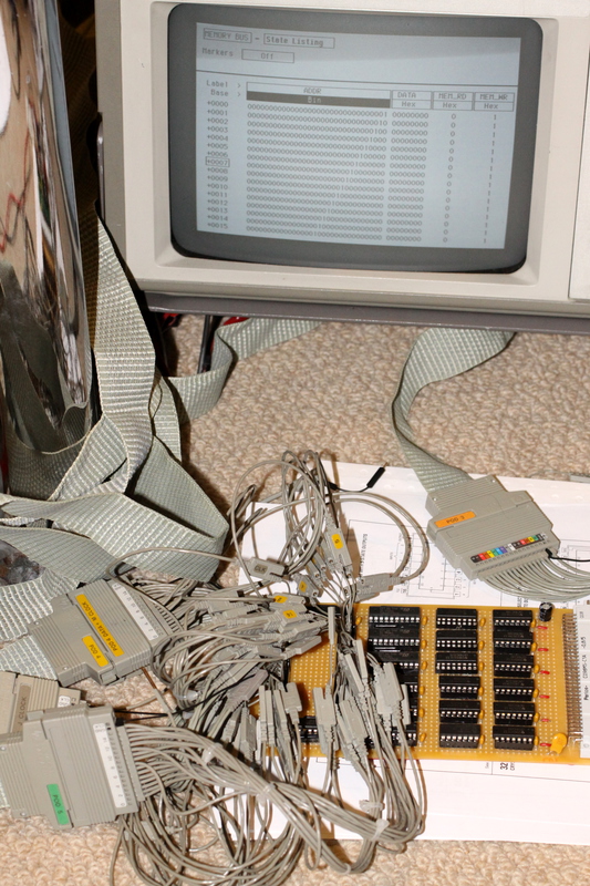 Yep, those bits are walking in the expected fashion!
Watching the state of the bus with no memory connected can only tell us so much, though — time to connect the RAM board and make sure practice agrees with theory. A few weeks back I'd performed a few basic memory transactions which all seemed to work properly, but to test it more thoroughly I put together another test loop on the mbed that writes random data to every location in RAM, then reads it back to make sure everything was as expected. That test passed first time, so to make sure it was actually testing something I tried running it again whilst occasionally shorting a data line to ground and changing the address of the RAM board (set via DIP switch). That caused the expected errors to appear, so everything looks good.
However, there is one thing I can't test using code running on the mbed to generate external stimuli, and that's how the memory system performs at a realistic target speed. Because I'm bit-banging the clocks, control signals and data in my test routines, it only manages to run tests at a few hundred kHz — an order of magnitude slower than the 'hopefully several MHz' clock speed I have in mind for the finished system. As a result, a memory cycle (from the point of view of a device on the bus) is almost 12 microseconds long, with three of those being the active period of the READ and WRITEx control signals. The Alliance AS6C4008s I'm using for RAM have worst-case timings of 55 nanoseconds, so I'm not even coming close to the sort of speeds where problems might start to show up.
That leaves me with a decision to make with regards which part of the design to concentrate on next. Building the clock generator board might let me test the memory system out at full speed, but the design I've prototyped for that uses a 4MHz crystal (based on the "I need a crystal and this 4MHz one was the first to come to hand" principle of part selection). It could well be a reasonable choice, but I should probably prototype the control unit first so that I know what my timings look like for instruction decode and issue...
... on second thoughts, maybe I should investigate whether I can get a faster clock out of the mbed by using its SPI peripheral support to drive the system's clocks instead of my belt-and-braces bit-banging. Hmm.