System/1 Build Log
An ongoing chronology of System/1's construction, and any other related musings.
8th March, 2018 - Shifty-looking characters hanging around (serial) ports
It's been a somewhat interesting start to the year here at BALJ Towers; the storms in January succeeded in bringing down my garden fence (which turned out to be reassuringly heavy when it came to rehanging it on fresh posts), then a snottogram arrived in the post threatening court action for non-payment of a parking ticket I'd already successfully appealed, quickly followed by a £1,200 water bill thanks to a leak in the meter pit back in October. Sorting that one out turned out to be somewhat less straightforward than expected, so by the end of February my pre-Christmas frustrations with System/1 had given way to a earnest desire to have a sufficiently quiet few days that I could get back to tinkering around with it!
Luckily the so-called Beast from the East intervened and deposited enough snow outside that I figured leaving the house would be an exercise in pointless masochism, especially since the pipework in my main en-suite had frozen up and I didn't fancy not being around in the event that it thawed and flooded the place. With a perfectly good excuse to spend a few days at home it seemed as good a time as any to sit back down and build the serial board — the symmetry with having drawn up the final schematics in snow in December was too good to resist.
The first step, as usual, was to plonk a decent handful of IC sockets down on a fresh Eurocard and come up with a sensible chip layout; usually this ends up with a couple of rows of sockets of uniform size, and then one row for oddball sizes (such as the DIP24 package for the MAX238, in this case). Any 74HC73s in the design also tend to get shoved off into one corner, as they have an irritatingly non-conformist approach to power pins; not only are they halfway down each side of the chip, instead of on opposite corners, but they have ground on the right and supply on the left instead of vice versa!
Once that's done and the various devices on the schematic have been renumbered to fit reasonably into the layout, I usually print off a working copy to cross connections off as I make them. This has turned out not to scale very well — it's fine for smaller designs where everything fits on one sheet and connections can be seen at-a-glance, but for recent boards I've found it error-prone when the same signal might appear in different sections of the design. Even with annotations to help, it can be easy to miss one connection in a run and have to patch it in later. I'd experimented previously with writing an EAGLE ULP (user-language program; EAGLE's scripting language does not apparently have a particularly snappy name) to generate wiring schedules from the schematic, but hadn't been too happy with the result. For the serial board, I decided to spend a little more time on the problem, and found the solution was to use the built-in netlist generator and then put together a Perl script to lightly massage the result into something more tailored for my purposes.
With the wiring schedule in hand, I could start work on the board; the IC sockets get soldered down first, at the same time as the power rails and decoupling caps — these hold the sockets in place by opposing corners (except for those 74HC73s!), although any pins which are tied high or low need to be taken care of at the same time or it can get a bit fiddly going back to add those ties in later. Then it was a simple matter of working down the wiring schedule, starting with the longest wiring runs (so that the shorter spans of wire can hold the longer ones down against the board); after a couple of wiring sessions I was making good progress. Then I noticed this:
System/1 construction update: who will win, three more pages of connections to solder or one spooly boi? pic.twitter.com/nN2EfSyRQk
— Ben A L Jemmett (@baljemmett) March 2, 2018
Luckily the solder reel lasted just long enough to finish wiring the entire board, which then passed QC first time in the form of buzzing it out against the wiring schedule (which again made things far easier than relying on the schematic — not sure why it took me so long to get around to adopting this approach!). After fitting the ICs and making up suitable IDC cables to connect it to the I/O board and the usual DE9/DB25 connectors on the RS232 side, everything looked to be working nicely — sending and receiving bytes via the front panel memory controls, reading the status registers, the various options available in the control register and even interrupts when data arrived or when there was room in the transmit FIFO all appeared to work first time. I felt somewhat cheated about this, as fiddling around with the test gear is half the fun of this project, until I noticed some weirdness when trying to send bytes as quickly as possible from a simple counting loop:
00 01 02 03 04 05 06 07 08 09 0A 0B 0C 0D 0E 0F
10 11 12 13 ... all counting normally until ...
20 21 22 23 24 25 26 27 28 29 3A 3B 3C 3D 3E 3F
30 31 32 33 34 35 36 37 38 39 4A ... you what?!
As each byte is split between two 4-bit-wide FIFO chips, it looks like this is the result of the two halves somehow getting out of sync; one of them is either removing entries from the queue when it shouldn't or failing to add new entries as they're written. The datasheet for the FIFO does suggest combining the status outputs when paralleling several chips to form a wider queue like this, which I had neglected to do because (at least on the CPU side) the delay between polling the status and then attempting to write to the device is going to be orders of magnitude longer than any skew between the two halves becoming ready to accept data. However, something has obviously gone wrong here, which means this was probably a false economy.
Rethinking my logic, I satisfied myself again that this was a reasonable choice for the receive FIFO — the UART can't really do anything other than stuff bytes into it as they arrive and hope for the best, so it doesn't pay any attention to the status signals beyond passing them on to the remote device for handshaking. On the CPU side of things, again, if there's data in one half of the FIFO when the status register is polled, there'll either be data in the other half already or it'll be in the process of bubbling up through the FIFO slots; by the time the FIFO is actually read, several microseconds down the line, this should be fine. The exception is if the buffer has overflowed at some point and a byte was received at a point where there was room in one half and not the other — but if the buffer has overflowed you've already lost!
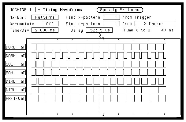
The transmit side is another matter, though. If the transmitter happens to check for queued data just as a byte is written, perhaps it'll have made its way to the front of one queue slightly before the other and so half the byte will be removed and the other half won't. This sounds somewhat plausible as an explanation for the observed issue — although the halves suddenly getting out of sync by five slots seems unlikely. Returning to the datasheet for the part and trying to make a bit more sense of some of the denser portions — it doesn't feature the clearest explanations I've ever read in a datasheet! — I notice that, despite it suggesting the SI (Shift In) signal is triggered by a positive-going edge, it also indicates that something 'interesting' might happen if SI is held high when the FIFO is empty; a circuit featuring several extra parts is provided to generate the correct status signals from multiple parallel FIFOs in this case. I can't easily implement that without awkwardly squeezing at least two more chips onto the board, but I can sit down with the logic analyzer and look at what those status signals are doing around the time we see odd output. It looks like the two are indeed getting out of sync; by the time the problem occurs the FIFO responsible for the high half of the byte claims to be empty except for the most recently-added byte, but the low one insists it's full except immediately after a byte is removed.
 I think I'm interpreting this correctly, anyway...
At this point I have three gates spare on the board — an inverter, a NOR and an OR — and at least two potential problems — the DOR (Data Out Ready) signals for the two FIFOs not being combined, thereby possibly allowing the transmitter to remove a byte when only half a byte is available, and the datasheet's intimations about holding SI high when the FIFO is empty. Since I'm driving that signal straight from the WRITE decoder, it does indeed idle high, expecting to clock data in at the end of every low-going pulse. Either or both of these points could be behind my data corruption, and with only three gates on hand I'm not sure which to prioritise; eventually, though, I noticed that I can combine the two DOR signals with the spare inverter and OR gate (I was already inverting one of the two outputs to get the AVAIL signal to the transmitter, and although I don't have a spare NAND to replace that inverter I can just apply De Morgan's laws to invert them both and OR the result instead). That leaves me with the spare NOR gate that I can wire up as an inverter to make the SI input idle low; that will mean shifting data into the FIFO at the start of a write cycle rather than the end, but the data bus will be steady by then due to the design of the memory interface and I/O boards. However, using all three spare gates means I won't then be able to do anything about the transmit FIFO status register as exposed to the CPU; we'll just have to rely on the earlier argument about the delay between checking and writing covering any skew between the two halves.
With crossed fingers and not much hope of success, I made the required changes to the board, hooked up the logic analyser again to catch any misbehaviour, and ran the test loop once more. Much to my surprise, the data corruption was gone; I'm not entirely sure which of the two fixes was most responsible for this, but my money's probably on the SI side. Either way, I'm happy, and it's probably time now to try bringing the machine up for some proper testing.