RAM Board
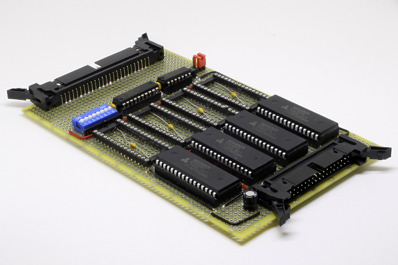 The RAM board, with 2MB populated in the lower bank.
The RAM board contains either 2MB or 4MB of SRAM, made up of one or two banks of four Alliance AS6C4008 512Kx8 devices apiece. Address decoding logic is included to allow the location of the board in the memory map to be changed by way of DIP switches; these specify eight bits of the address where the board's memory appears.
A jumper allows the two banks to either appear contiguously in the RAM region of System/1's memory map, or alternatively to map the second (upper) bank in the ROM region to allow it to be used as a 'fake ROM' when developing the system's firmware.
The board does not currently assert the WAIT line on the memory bus at all; in the unlikely event that the processor ends up able to be clocked at a high enough speed that the RAM's cycle timing requirements are violated, I may have to retrofit a suitable one-shot circuit to cause the clock generator to insert sufficient wait states.
Related Build Log Entries
- 17th January, 2015 - Adventures in the removal of flux residue
- 18th January, 2015 - Populating and testing the memory interface
- 7th February, 2015 - More memory interface testing