Memory Interface
 The memory interface board
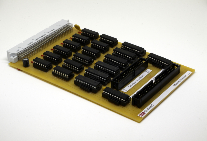
The Memory Interface board consists of the memory address register (MAR), memory data register (MDR), and control logic for both the registers themselves and the control signals carried on the memory bus.
Each of the registers is made up of four 74HC299 universal shift registers, giving a 32-bit shift register that supports both serial and parallel input and output. My original sketches had the MAR being constructed from 74HC164 devices, since it is clocked from the BIT_CLK signal which idles during memory operations — and thus would leave the address bus stable during a memory access — except for an oversight revealed whilst prototyping it on a breadboard which caused the support for reading single bytes from memory to be completely broken. This flaw in the original design (hey, that's what the breadboard's for, after all!) could be fixed easily enough by switching to '299s, or slightly less easily by inserting an additional latch. Using the '299 for both registers seemed the more consistent design.
In addition to the two registers, the memory interface has control logic to support reading and writing 32-bit words (always aligned to a natural address, i.e. a multiple of 4 bytes), and 8-bit bytes at any memory location (with reads supporting optional sign extension to 32 bits). It also buffers the INT_CTX and RESET signals onto the memory bus, and handles the pulling-up and inverting of WAIT and IRQ bus lines — these lines are intended to be pulled low by devices on the memory bus to indicate that a memory transaction needs to be extended (to meet timing requirements) or to request an interrupt.
To simplify the logic required to support byte-oriented writes on each board attached to the memory bus, the memory interface produces four write strobes (WRITE0 to WRITE3) which are associated with writes to each of the four sub-bytes of the full 32-bit data bus. Reads are always performed at the full 32-bit width, but half of a 74HC153 1-of-4 data selector is used to select which of the four bytes of the MDR should be read out in the case of a single-byte read.
A second 74HC153 is then used as two independent 1-of-2 data selectors, with one half used to switch between the first eight bits from the MDR and either a latched copy of the most-significant bit (for signed byte reads) or zeroes (for unsigned byte reads); when a full word is being read, the entire MDR contents are passed through without any switching. The other half of that '153 is used similarly when writing a single byte, and feeds the MDR with four copies of the first eight bits of data. This allows that one byte to appear in all four sub-bytes of the data bus, so that when the appropriate WRITEx line is asserted only the appropriate memory location is updated. When a full word is being written, it is loaded into the MDR as-is and all four WRITEx lines are asserted simultaneously.
Related Build Log Entries
- 16th November, 2014 (backdated) - Prototyping the memory interface
- 17th December, 2014 (backdated) - Memory interface built
- 17th January, 2015 - Adventures in the removal of flux residue
- 18th January, 2015 - Populating and testing the memory interface
- 7th February, 2015 - More memory interface testing