System/1 Build Log
An ongoing chronology of System/1's construction, and any other related musings.
15th August, 2017 - Building the clock board
Unfortunately it took a little longer than I would have liked to find the time to build the clock board; after I'd finished tinkering with the schematic, debating which signals made the most sense to bring out to the debug header I wanted to include, and fiddling with chip/gate assignments in search of the elusive 'good' board layout, I decided it made sense to wait until I had a few solid days free to finally build the board. The wiring involved for this one, like most of the recent boards, is on a rather labour-intensive scale, and experience tells me it makes more sense to be able to sit down for a good few hours at a stretch to get into a rhythm with the wiring pencil rather than scrape an hour or so here and there in the evenings.
A suitable opportunity presented itself at the end of July, when I had a couple of weeks' holiday; wiring it all up took about 12 hours over a couple of days, with remarkably few mishaps along the way. A continuity test to cross-check all the connections against the schematic passed with only a couple of minor touchings-up required, so I moved on to populating the IC sockets and testing the board out in isolation. Since the design broke down quite cleanly into distinct sections, it seemed sensible to do this in stages; the first was to fit the quartz crystal and check the oscillator itself ran, which showed a nice clean 4MHz signal with the various divider taps all present and correct.
After installing the frequency selection jumpers and testing the operation of the clock source selector — the design allows for an external switch to select between two crystal-derived clocks and two external clocks, intended for debugging or blinkenlights purposes — I moved on to testing the machine cycle state machine. This again worked nicely, and the debug header made it easy to connect the logic analyzer up and make sure it was correctly responding to the various control signals that the control unit and front-panel controller might generate.
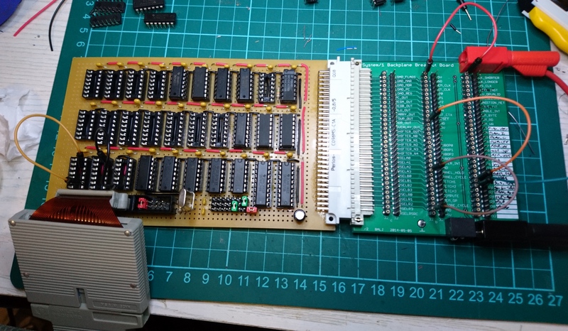 Testing the oscillator and state machine.
Adventures in inventory mismanagement...
Moving on to the interrupt logic, I hit a minor snag — the generation of the final INT_CTX signal depends on a 74HC10 triple 3-NAND chip, and not only did I not have one in stock but I apparently had never had any in stock to start with! I initially took this to suggest only that I must have introduced the part to the schematic when trying to optimise the number of chips or gates required somewhere, but looking more closely it became apparent that both places I was using it were places that I'd made a change to the design without testing it on the breadboard first. This was not comforting news... Even worse, I made this discovery on a Saturday evening, so it looked like progress would grind to a halt until at least Tuesday — Farnell's next-day delivery is usually very reliable, but they won't take an order on Saturday night for Sunday delivery!
Luckily, though, just as I was contemplating breaking out a heavy-duty sulk, it occurred to me to check what time my local Maplin closed. Their website didn't list the 74HC10, but did claim the 74LS10 version was in stock in Banbury — and I'd have about five minutes to spare if I set off immediately. Grabbing a handful of change and my car keys, I got there just in time to secure the last one from their parts drawer; on the drive home I began to get a sneaking feeling that 74LS and 74HC parts were sufficiently incompatible in terms of voltage levels to cause a problem, but reasoned that I could probably put it on a breadboard and wire it up via whatever 74HCT parts I had on hand to act as level translators. In the event, though, this turned out to be unnecessary; the LS part dropped right in with no obvious objections from the downstream gates. Not great practice, admittedly, but it'd certainly do until I could get hold of the right part.
With that chip in place, and some creative jumper wiring on the backplane breakout board I use for testing individual boards in isolation, I tested out the three interrupt sources (bus, front-panel and NMI) and found they all appeared to trigger an appropriate reaction — at least, once I remembered that I needed to strap the ENABLE_INT line high and pulse the LEAVE signal (both generated by the not-yet-populated 74HC259 addressable latch) before the two maskable interrupts would be recognised. By this stage I also had enough of the circuit populated for the new 'read status word' instruction to be decoded, so I fitted the multiplexers that generate the status word and made sure the resulting bitstream correctly reflected the interrupt state.
... and falling at the last hurdle
The last section of the board to test was the addressable latch that implements the SYSOP instructions. Since everything so far had worked as expected, I had high hopes as I fitted that final chip — all the supporting gates already being present as part of the previous sections — and worked my way down the possible combinations of SUBOP bits representing the various instructions. The latching bits looked to be working fine, with the ENABLE_INT and MANIPULATE_USER_MODE bits plus two spare bits I brought out for diagnostic purposes all setting and clearing in response to the corresponding instructions. Working down the four 'pulsing' instructions — TRAP, HALT, WAIT (which halts execution but only until the next interrupt) and LEAVE — I found the first three appeared to work fine, but although the LEAVE instruction correctly cleared INT_CTX it also seemingly prevented any later interrupts from being serviced. Although an ENTER_INT cycle was requested and executed, before the next instruction cycle could commence the INT_CTX line would drop low again.
A little poking around with the logic analyser revealed the root cause to be good old-fashioned hubris, in the form of one of those untested changes I'd made when fiddling with the schematic. For bonus should-have-seen-that-coming points, it even managed to involve that 74HC10 part I'd added; although I was already using one gate in the chip to generate INT_CTX, I'd noticed that I could use another in place of a standard 2-input NAND that generated the enable signal for the addressable latch. That would give me an extra input which could be used to disable some SYSOP instructions when not in interrupt context. This was basically a 'hey, I have some gates spare so it's free!' approach to a supervisor bit, to provide some sort of separation between OS-type functionality and user-level code; I still don't know if this is even a good idea, to be honest, but I'd added it anyway...
This extra gate simply partitions the SYSOP instructions based on the third SUBOP bit; since the fourth bit is used to decide whether a signal is latching or pulsing, this ends up splitting those groups further into 'interrupt-context only' and 'always available' sets. The signals I'd intended to prevent user-mode code from accessing were HALT , ENABLE_INT and MANIPULATE_USER_MODE, but since I needed two bits of each type for this trick to work I had to choose an additional pulsing bit to protect similarly. LEAVE had seemed to be the sensible choice, since it would effectively be a NOP for user-mode code anyway.
What I hadn't realised before testing the finished board was that asserting the LEAVE signal causes the INT_CTX signal to be cleared on the next clock edge, thereby leaving interrupt context immediately and, crucially, disabling any further change to the state of the LEAVE line — including returning it to 0 towards the end of the same instruction cycle. Therefore the LEAVE line remained high and would cause the INT_CTX flip-flop to be continuously reset on every clock edge; the only way to escape this state and allow interrupts to execute again was to clear the addressable latch (and every other register in the machine) by asserting RESET. Whoops!
A board isn't complete without a bodge on the back
Once I'd finished grumbling at myself for being a wally and instead started thinking of a suitable fix, it struck me that simply ORing the LEAVE bit with the INT_CTX signal before it reaches the privilege check should work — we'd effectively stay in interrupt context until the LEAVE instruction had done its work and deasserted the bit in the addressable latch. Unfortunately there weren't any spare OR gates on the board (in fact, there aren't any unused gates on it at all!), nor was there room to fit an extra 74HC32 chip. One option would be to use a surface-mount 74HC1G32 device, which would provide a single OR gate, so I added a handful of those (along with the other basic logic gates in their 1G variants, just in case) to my Farnell order along with all the other chips I'd not had on hand and resigned myself to gluing one to the bottom of the board and wiring it up dead-bug style.
Shortly afterwards, when pondering the indignity of having a single surface-mount part amidst the sea of DIP chips making up the processor, I realised there was another option that might work just as well — a diode OR. Even better, since I'd noticed it would be less disruptive to OR LEAVE with the output of the privilege check rather than the input, I could even test this idea by bending the relevant input pin on the 74LS10 out of its socket and then using some test clips and jumper wires to connect a diode and resistor to the appropriate input signals. To my vague surprise, this ungainly mess of nonsense worked perfectly first time, so with the aid of a couple of lengths of heatshrink to avoid short-circuit-related mishaps I installed the two new parts on the back of the board permanently.
With that done, the board passed all the tests I could think of throwing at it when it was sitting on the desk in isolation; it was time to plug it into the backplane and find out if it could drive the rest of the machine properly. The basic front-panel operations appeared to be working properly, which was a good start, but code wouldn't run; by chance I noticed that flipping the register display between the MDR and another register would cause the bits in the former to shift along one place, which sounded suspiciously like the problem caused by the weak pull-up resistor on the LOAD_MDR line that I'd already identified when prototyping this board. It turned out the resistor I'd temporarily added to the backplane breakout wasn't particularly securely gripped by the sockets it was in and reseating it cured this problem, at least running on a 2MHz clock; at 4MHz it was still intermittently showing up, so making a note to revisit this later I switched to the lower clock frequency for the rest of the initial testing.
The machine could now run some simple test code properly, but wasn't responding to the HALT or TRAP instructions. This lead me to discover that the IRQ and SYSOP lines, from the memory interface and control unit respectively, weren't connected to the slot the clock board lives in; when I'd wired up the backplane I must have left them until I was sure which board was going to end up responsible for those functions. Once those connections had been made the various SYSOP instructions started working as anticipated, but that in turn revealed that the interrupt logic was occasionally firing without any obvious cause. Unfortunately, the spacing of the slots on the backplane make probing chip pins on the board almost impossible unless they're very near the edge, and also render the debug header I'd connected the logic analyser to earlier completely inaccessible, so it looks like I'm going to need to build myself an extender card to get better access to the board before I can make any further progress!