System/1 Build Log
An ongoing chronology of System/1's construction, and any other related musings.
25th July, 2015 - Debugging the control unit, and running System/1's first code
All my prototyping and testing so far has revolved around individual modules in the system — building each one up as a breadboard prototype to make sure the design is good, then testing each board as the prototype is turned into a finished module. This is fine, as far as it goes, but of course at some point it would be a good idea to make sure they work together as intended — preferably before committing complex pieces of logic like the control unit to their final form!
To that end, I spent a few hours this week connecting the prototype control unit (as seen last time) to the functional units that have been assembled so far. The first step in doing this was wiring up the backplane board; I'm using a VMEbus J2 backplane from Vero, which has ten female DIN41612 connectors with row b bussed across (and various pins wired to the power planes); rows a and c are left uncommitted, for the user to wire up as required. This is done using the male connectors on the back of the board, which have connector bodies that can be removed in order to connect the pins together using proper old-school wire wrapping.
Since this leaves 64 uncommitted signals, times ten slots, I didn't much fancy bussing them all across the entire backplane. I'd tried to keep all the signals that are needed by several boards on row b, and making a list of which boards need to drive or consume the remaining signals gave a much less daunting list of around 60 connections to make. However, by only partially wiring up the backplane, the various boards are constrained to operate only in slots with suitable wiring, which could lead to exciting forms of brokenness should they accidentally end up in the wrong place at any point!
To help avoid such mistakes, it occurred to me that a set of pins could be dedicated to a 'slot ID' function, which lights a status LED on the plugin boards when they're in the correct slot. Using eleven pins for this seemed a bit excessive, as it chews up nearly all of the spare pins I have left, but luckily a recent redesign of the shifter module means I no longer need the five 'shift distance' pins SHIFTER_N0-4. Five pins gives ample room to arrange ten combinations of +5V and GND to achieve the desired effect, and it's just the right size wire-wrapping job to let me practice the technique before I start on the main bus.
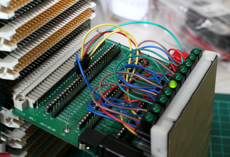 Testing the slot ID pins after wiring.
With that practice run complete with only a small amount of swearing and fiddling around to remove mistaken or duff wraps, it was time to move on to the important signals. This took a little longer, but after getting into a rhythm it proved straightforward enough:
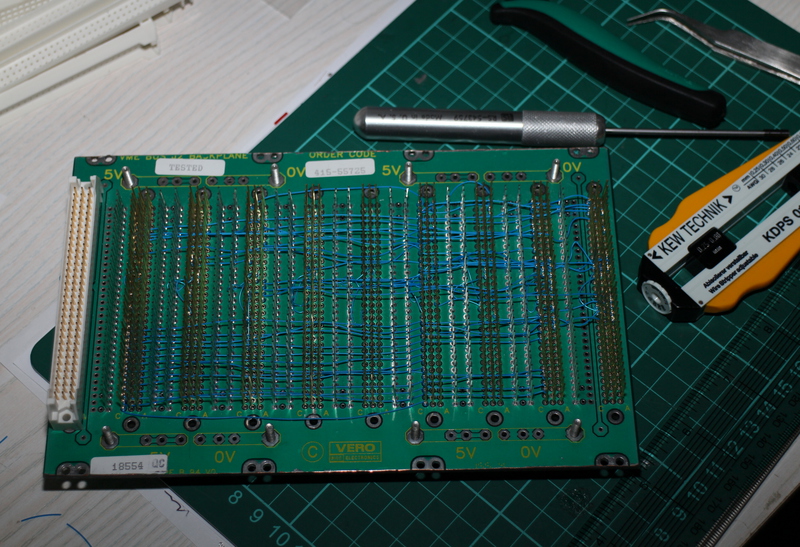 The backplane after a couple of hours of cutting, stripping and twiddling wires.
With the functional units now all theoretically able to communicate with each other and the rest of the system, I could hook my backplane breakout board up to the back of the slot that the control unit will live in and bring the relevant signal lines out to the pile of breadboard and spaghetti that implements the prototype. This placed a severe strain on my stock of breadboard jumper wires, but in the end I had just enough to bring the relevant signals close enough to the backplane for a bunch of solid-core hookup wire to bridge the gap...
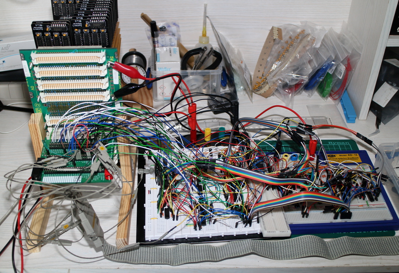 Behold the horror!
That done, it was back to the mbed to write another set of test routines; this one has to pretend to be a combination of the clock generator, front panel and memory interface boards, so that it can inject instructions to run whilst generating the expected clock and machine cycle signals and also interrogating the state of registers between instructions. The first attempt seemed to be a reasonable start, if not exactly brilliant — the program counter was incrementing properly between instructions, and operations on register 0 appeared to work properly, but other registers seemed to contain nonsense and the interrogation routine was generating spurious memory accesses — but a bit of head-scratching revealed that I'd miscounted bits in the instruction word layout and the register interrogation code was accidentally putting the desired register number in the opcode field rather than the source/destination fields. Whoops. Never trust C code that compiles first time!
With register interrogation and injection of single instructions working, testing the instruction set proceeded quickly; there were two wiring mistakes in the instruction word register (I'd forgotten to connect the immediate field's output to the bus routing section of the control unit, so instructions that used an immediate operand would find themselves operating on floating garbage instead — usually all-ones — and then once that was put right I found I'd also left one of the control pins on the bottom half of the register floating so that it would sometimes fail to shift the data out at all!), but they were easily corrected if not so easily diagnosed. That left one unfortunate problem which had crept in unnoticed as I was laying out the instruction set originally; the encoding for a store-to-immediate-address instruction uses the immediate field for the address, but also needs the B register operand field to specify the register from which data should be stored. Unfortunately that field overlaps the top four bits of the immediate field, resulting in a store-utter-nonsense-to-immediate-address instruction; not hugely useful.
Because the memory data register can only be loaded from the B bus, there's no way to tweak the instruction decoding to use the A register for the data instead; nor was it possible to swap the A and B operand fields entirely, because other instructions are being correctly decoded as 'A and either B or immediate field'. This realisation probably marked the point of peak profanity in the project to date, surpassing even the several days I spent chasing a problem caused by forgetting to turn the power supply down to 3.3V when using the mbed.
Luckily an answer suggested itself shortly after I'd finished turning the air above my bench blue, and by introducing one extra '157 quad 2:1 mux I can effectively swap the A and B register operand fields for selected instructions. This works by swapping not the two four-bit-wide RSELAn and RSELBn register selection fields themselves, but rather the REGA_OUT and REGB_OUT outputs from the register file before they're connected to the A and B buses by the operand routing logic. This allows the A operand field to select a register for the B bus, and vice versa, without needing to change any of the main control signals for routing operands onto the buses.
With the extra muxes in place, all of the store instructions now behave properly; however, only swapping the two source operand fields for store instructions introduces a peculiar wart where they read as 'store A to address B or immediate' but loads read as 'load R from address A or immediate'. Fortunately I already have a signal in the control unit that represents 'load or store instruction', so using that to control the new muxes instead makes the addressing options for both memory access instructions consistent with each other. Two related oddball encodings are much nicer than one oddball encoding, at least as far as 'not looking like a last-minute bodge' goes...
Having shaken that last wart out, and being very glad that I bothered to wire the prototype control unit up to the backplane for a full test rather than just relying on the generated control signals matching what my notes suggested would be needed, it was time to write a short program to see if the thing could actually run code as intended; generating the Fibonacci sequence iteratively seemed a reasonable test, if somewhat obvious, and so to quote the mbed:
/reset/run
Register state after reset:
r0=0x00000000    r1=0x00000000    r2=0x00000000    r3=0x00000000
r4=0x00000000    r5=0x00000000    r6=0x00000000    r7=0x00000000
r8=0x00000000    r9=0x00000000    ra=0x00000000    rb=0x00000000
rc=0x00000000    rd=0x00000000    re=0x00000000    rf=0x00000000
pc=0x00000000


/fib/run 46
Memory word write, MAR = 0x0000fff0, MDR = 0x00000001 (1)
Memory word write, MAR = 0x0000fff0, MDR = 0x00000001 (1)
Memory word write, MAR = 0x0000fff0, MDR = 0x00000002 (2)
Memory word write, MAR = 0x0000fff0, MDR = 0x00000003 (3)
Memory word write, MAR = 0x0000fff0, MDR = 0x00000005 (5)
Memory word write, MAR = 0x0000fff0, MDR = 0x00000008 (8)
Memory word write, MAR = 0x0000fff0, MDR = 0x0000000d (13)
Memory word write, MAR = 0x0000fff0, MDR = 0x00000015 (21)
Memory word write, MAR = 0x0000fff0, MDR = 0x00000022 (34)
Memory word write, MAR = 0x0000fff0, MDR = 0x00000037 (55)
Memory word write, MAR = 0x0000fff0, MDR = 0x00000059 (89)
Memory word write, MAR = 0x0000fff0, MDR = 0x00000090 (144)
Memory word write, MAR = 0x0000fff0, MDR = 0x000000e9 (233)
Memory word write, MAR = 0x0000fff0, MDR = 0x00000179 (377)
Memory word write, MAR = 0x0000fff0, MDR = 0x00000262 (610)
Memory word write, MAR = 0x0000fff0, MDR = 0x000003db (987)
Memory word write, MAR = 0x0000fff0, MDR = 0x0000063d (1597)
Memory word write, MAR = 0x0000fff0, MDR = 0x00000a18 (2584)
Memory word write, MAR = 0x0000fff0, MDR = 0x00001055 (4181)
Memory word write, MAR = 0x0000fff0, MDR = 0x00001a6d (6765)
Memory word write, MAR = 0x0000fff0, MDR = 0x00002ac2 (10946)
Memory word write, MAR = 0x0000fff0, MDR = 0x0000452f (17711)
Memory word write, MAR = 0x0000fff0, MDR = 0x00006ff1 (28657)
Memory word write, MAR = 0x0000fff0, MDR = 0x0000b520 (46368)
Memory word write, MAR = 0x0000fff0, MDR = 0x00012511 (75025)
Memory word write, MAR = 0x0000fff0, MDR = 0x0001da31 (121393)
Memory word write, MAR = 0x0000fff0, MDR = 0x0002ff42 (196418)
Memory word write, MAR = 0x0000fff0, MDR = 0x0004d973 (317811)
Memory word write, MAR = 0x0000fff0, MDR = 0x0007d8b5 (514229)
Memory word write, MAR = 0x0000fff0, MDR = 0x000cb228 (832040)
Memory word write, MAR = 0x0000fff0, MDR = 0x00148add (1346269)
Memory word write, MAR = 0x0000fff0, MDR = 0x00213d05 (2178309)
Memory word write, MAR = 0x0000fff0, MDR = 0x0035c7e2 (3524578)
Memory word write, MAR = 0x0000fff0, MDR = 0x005704e7 (5702887)
Memory word write, MAR = 0x0000fff0, MDR = 0x008cccc9 (9227465)
Memory word write, MAR = 0x0000fff0, MDR = 0x00e3d1b0 (14930352)
Memory word write, MAR = 0x0000fff0, MDR = 0x01709e79 (24157817)
Memory word write, MAR = 0x0000fff0, MDR = 0x02547029 (39088169)
Memory word write, MAR = 0x0000fff0, MDR = 0x03c50ea2 (63245986)
Memory word write, MAR = 0x0000fff0, MDR = 0x06197ecb (102334155)
Memory word write, MAR = 0x0000fff0, MDR = 0x09de8d6d (165580141)
Memory word write, MAR = 0x0000fff0, MDR = 0x0ff80c38 (267914296)
Memory word write, MAR = 0x0000fff0, MDR = 0x19d699a5 (433494437)
Memory word write, MAR = 0x0000fff0, MDR = 0x29cea5dd (701408733)
Memory word write, MAR = 0x0000fff0, MDR = 0x43a53f82 (1134903170)
Memory word write, MAR = 0x0000fff0, MDR = 0x6d73e55f (1836311903)
Terminated at PC >= 0x0000fff0
I call that a successful test. Happy days!