System/1 Build Log
An ongoing chronology of System/1's construction, and any other related musings.
1st October, 2016
When it was time to move the front panel controller to a soldered board, I decided to abandon the experimental wiring styles that I'd used on the control unit and the signal conditioning boards, despite both of those being similar in chip density to the new one. On those board I'd run the power rails on the solder side, as bare copper 'bus bars' of 1/0.6mm plating wire running either across the rows or down the centre of each column of chips; although this did dramatically reduce the effort involved in getting power to each chip, it turned out to be a absolute pain in terms of running signal wiring over the top. In some cases, even just wrapping the wire around a pin became a problem due to the obstruction — in others, the bare rail wiring ended up a little too close to a nearby solder joint, with the inevitable bridges needing to be cleaned up afterwards.
With this in mind I went back to my previous wiring method involving short jumpers between the decoupling caps above each chip, and others bringing the ground down from the caps to the chips' ground pins. Although considerably more labour-intensive — it took several multiple-hour sessions at the bench just to get the power wired this time — it did end up being a much more pleasant build overall. It would have been wise to check whether I was correctly remembering which orientation I'd built all the existing boards in, though...
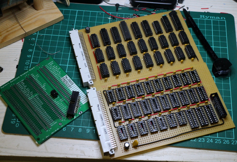 Spot the difference: the control unit is on top, the new board with its power wiring nearly complete below.
From here, construction proceeded apace, and after a few evenings I had a complete front-panel controller board ready to plug into the backplane. Alas, when I first wired up the uncommitted pins on the backplane I hadn't yet finished the design of this board, so several signals it needs to operate weren't yet routed to the correct slot. However, since the mbed code I've been using to generate test signals simulates a combination of the clock generator and memory controller boards in order to force the system to dance to a suitable tune, I decided it made sense to install the front-panel controller in place of the (absent) memory controller and use jumper cables to patch in the handful of extra signals temporarily. With this done, I started the initial testing of the front panel subsystem — only to be met with abject failure.
Having decided that "absolutely nothing is working" was completely useless for diagnostic purposes, albeit an accurate first approximation of the situation, I set about trying to narrow this down into a list of actual problems. First up, although the display seemed to accurately reflect changes to register contents if they were caused by the machine executing code (as opposed to operator requests via the front panel), it wouldn't react to changes of the selected register — instead, the controller would continually request that the register be reloaded from itself, which is how it ensures the displayed data is accurate after a selection change. It was also somewhat suspicious that I couldn't deposit data into registers from the front-panel switches; although the deposit request would be honoured, it was hit-and-miss whether the resulting value reflected the switch settings or not. Thinking about this further, the common factor linking these problems was the DEP_LATCH signal, which controls when the front-panel data and register-selection switch settings are latched; this was active-high leaving the front-panel controller board, but was an active-low DEP_LATCH signal on the signal conditioning board and input registers! A couple of bodge wires to add a spare inverter to that line before it left the controller corrected that oversight, and fixed most of the these issues; data could now be deposited reliably in at least some registers, although it would still occasionally get stuck in a loop after the register selection changed.
Trying to work out why only some registers could be updated proved to be an exercise in frustration, especially since the logic analyser claimed all the signals looked fine leaving the controller board, and after a few debugging sessions with no progress I turned my attention instead to solving the issue with changing the register selection. Double-checking the state the front panel controller was in when it got stuck revealed it was indeed requesting one of the aforementioned 'reload' operations, and that this wasn't spurious — the priority encoder that chooses a pending supervisory function to execute was really seeing a 'reload required' input. This input can be generated in one of two ways; automatically by a flip-flop on the controller (triggered by a memory-read operation from the front panel when the memory data register is selected for display, so that the newly-read data is displayed to the operator), or whenever the signal conditioning board asserts a SEL_CHANGED signal. That board remembers the selected register each time new data is latched into the front panel, and signals a change whenever that state differs from the current settings. Tracing these two possibilities back showed that it was the latter case; although the controller seemed to be signalling appropriately for the relevant register to be reloaded, it wasn't noticing the operation happening and thus was failing to update the display.
Since correctly reloading a general-purpose register requires nine signals to be in the right state (four RSELAn source register selection bits, four RSELRn destination register selection bits, and the overall LOAD_REG signal) and the other registers require just one (either LOAD_PC, LOAD_MAR or LOAD_MDR) it seemed like a good idea to concentrate on one of the latter set. Of those the MAR register looked like the best choice since it can also be incremented using the front panel's 'next address' button as well as by single-stepping through program code. Experimenting with these options showed that the display was reliably updated in both cases, which eliminated the display update logic and the LOAD_MAR driver from the investigation — the problem must lie somewhere in the deposit/reload logic itself.
Watching the signals involved in loading registers for these two operations with the logic analyser didn't prove very fruitful, as although the signals enabling the various LOAD_* drivers were obviously not being asserted reliably the inputs to the 74HC139 decoder that generates them looked fine. I don't think I've suffered a faulty chip yet in this project (and I didn't have a spare to hand anyway!) so it was time to dig out the oscilloscope for a look beyond the logic analyser's digital view of the world, and sure enough it turned out that when the controller got stuck in a reload loop the active-low signal enabling the decoder was only dropping to half the rail voltage. This was low enough to register as a 0 according to the LA's default threshold setting (oops), but not low enough for the decoder to recognise. Checking the various pins that signal connects to revealed one likely candidate for problems — it connects to pin 19 on a 74HC244 bus driver, which is right next to the positive supply on pin 20 — but inspecting and reworking that connection just in case didn't solve the problem. Unfortunately chasing the relevant wire around the board didn't find it straying close to the positive rail at any other point, either, but after some very close inspection and cross-referencing the culprit was eventually identified — it had rubbed against an unused nearly-always-high pin on the '139 decoder, causing an intermittent short through that device to the positive rail. Tugging it away from the pin as a quick test allowed the enable signal to properly assert and trigger the required register load, so a touch of nail varnish around the wire to bolster the damaged enamel solved that stuck-in-a-loop problem — hopefully once and for all!
System/1 construction update: can't sleep, logic analyser will eat me... can't sleep, logic analyser will eat me... pic.twitter.com/gqAbf3ZQO7
— Ben A L Jemmett (@baljemmett) September 22, 2016
It all seems so straightforward after the fact, but it took a week of hair-pulling and this sort of nonsense to figure out where to apply that nail varnish...
With most front-panel features now behaving properly after correcting that short, there was one spot of weirdness remaining — not all of the general-purpose registers could be viewed or modified successfully. In fact, sometimes a register would be overwritten with the values from a different register when the selection was changed. This time, chasing the selection lines from the front panel through the controller showed everything was correct right through to the output of the buffer on the RSELA0 line, which was stuck low. That definitely explained why registers were getting overwritten occasionally, but not why the display wasn't updating when some registers were changed from code. Digging further into the system, all of the other RSELAn and RSELRn lines looked correct leaving the front-panel controller board when it was driving them — it wasn't until I attached probes to the corresponding inputs on the register file board that I noticed I'd somehow managed to patch that whole set of pins in off-by-one when pulling them from an available backplane slot. Serves me right for cutting corners and not installing the additional backplane wiring properly when setting up the test rig!
 It may look like a mess of test wiring and probe connections, but underneath those lies success.
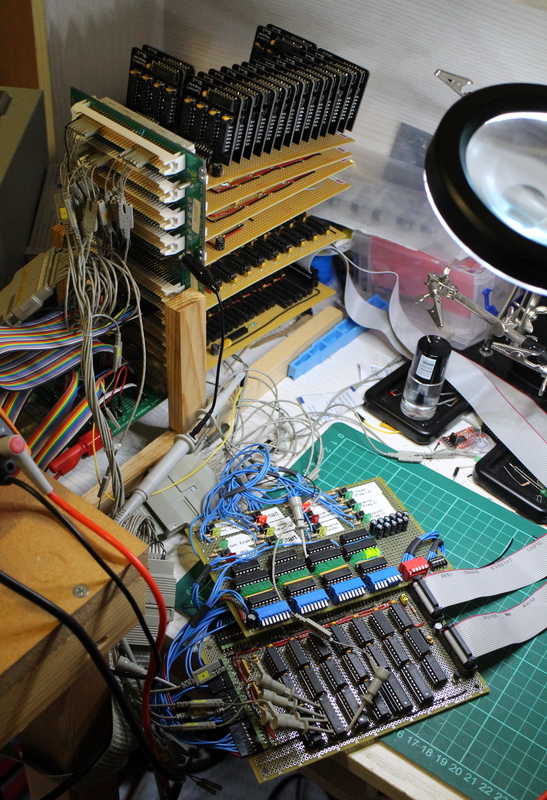
Finally, after what felt like far too many evenings squeezed into the corner between my study desk and the temporarily-repurposed enlarger table that was home to the logic analyser and oscilloscope, I had a working front panel and controller board. Next up, a little carpentry to offer some much-needed support to that register file board, then onwards to the clock generator!
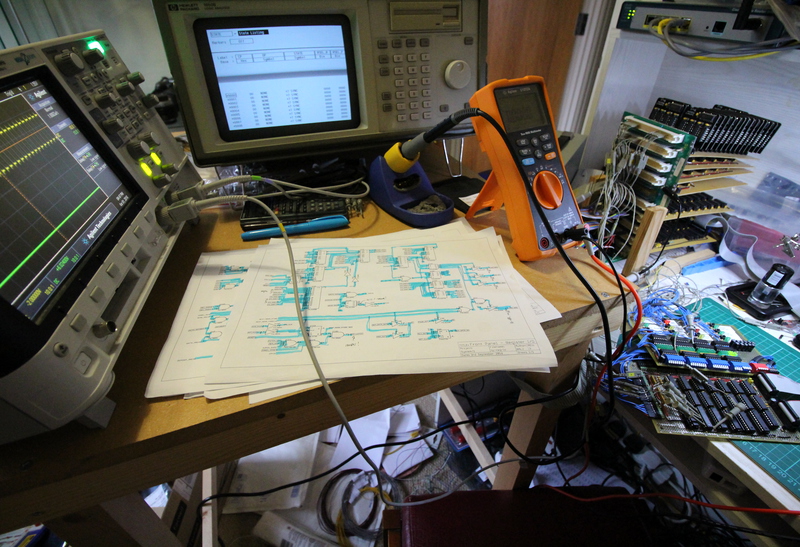 It certainly will be nice to have room to move again!
(OK, I just wanted an excuse to try out my new ultrawide lens...)