Main Register File
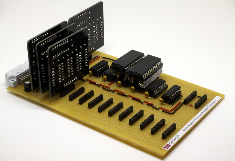 The half-populated Main Register File board
The Main Register File and Program Counters board contains, as the name suggests, the sixteen general-purpose registers and two program counter registers (one each for code execution in normal and interrupt contexts.)
Each of the eighteen registers is implemented as a plug-in module consisting of a 32-bit shift register and logic to either circulate the existing data or replace it with new data as the contents are shifted out.
The main register file is controlled using a 74HC4514 4-to-16 decoder to generate individual LOAD signals for each register, and two 74150 1-of-16 data selectors to read data out of the appropriate registers. Because the '150 is not available as a 74HC device — at least, not that I could find when ordering the bulk of the components — the plain TTL variety is used. Since the output of the '150 is a negated version of the selected input, an output inverter is required for each selector; using a 74HCT06 hex inverter for this purpose ensures that the TTL outputs can be made compatible with the CMOS levels used in the rest of the system.
Half of a 74HC153 dual 1-of-4 data selector is used to select whether register data should be loaded from the R or B buses, based on the REGSELRSRC signal; the other half is used to select which of the two program counters is currently in use. In addition, half of a 74HC08 quad AND and one of the spare gates from the hex inverter are used to generate the LOAD signals for each of the two program counters based on the state of the LOAD_PC and INT_CTX signals.
Register Operations
Using the RSEL* signals on the backplane connector, the system can select any two registers to read out — the data appears at REGA_OUT and REGB_OUT, ready to be selected onto the A and B buses as required — and select any one register to be loaded with data from the R or B buses. This is controlled using the LOAD_REG signal.
The program counter registers are arranged such that only one is accessible to the system at a time; which one this is depends on the state of the INT_CTX backplane signal. The current PC contents are always made available via the PC_OUT signal, with the LOAD_PC signal being asserted to load the PC from the R bus.
Individual Register Modules
Each module comprises four 74HC164 8-bit shift registers, cascaded to form a 32-bit shift register, with a 74HC157 data selector used to switch the input (at the MSB end of the register) from either the register output or the IN pin of the module depending on the state of the LOAD pin. Data from the register output (the LSB end) is always presented on the OUT pin, with CLK and CLR signals, power and ground rails making up the remaining module pins.
The (insultingly simple) schematic for the individual register modules is linked alongside the main register file schematic at the top of the page. (Note that this schematic has not been updated since I first started formalising my ideas for System/1, and so the signal names don't quite line up with those on the main register file schematic!)
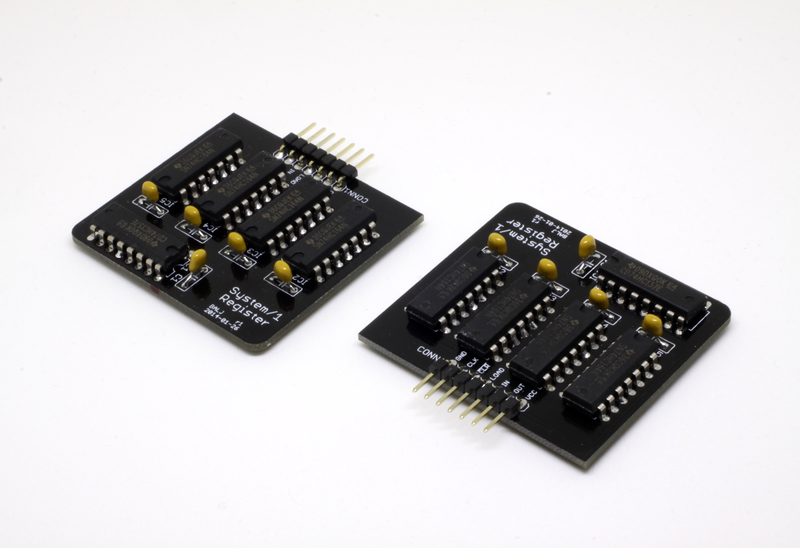 A pair of completed register modules
The individual modules are built on small PCBs, rather than sticking to the prototyping boards used for the rest of the system; since I need at least eighteen of the modules, and wiring them up by hand would be mind-numbingly tedious, it seemed somewhat daft not to simply throw a few quid in the direction of Elecrow to have 20 boards made up ready for the start of construction!
Related Build Log Entries
- 18th April, 2014 (backdated) - Construction begins!
- 8th June, 2014 (backdated) - Full set of register module boards assembled
- 14th June, 2014 (backdated) - Populating the register file
- 20th June, 2014 (1) (backdated) - Populating the register file, take 2
- 20th June, 2014 (2) (backdated) - Initial register file testing
- 13th July, 2014 (backdated) - Main Register File testing completed